Pulse duration: 15ns
Wavelength : 157nm
Max energy : 55mJ
Max repetition rate : 20Hz
The VUV absorption spectrometer is operating over the spectral range from 110 to 200 nm. It consists of a hydrogen lamp operating in a longitudinal stabilized discharge mode, a stainless steel vacuum chamber and a VUV monochromator (Acton VM502) equipped with a solar-blind photomultiplier (EM1 9412). It is also equipped with liquid nitrogen and a closed cycle helium cryogenic facility (CTI-Cryogenic) for measurements at low temperatures (8-275 K). The high signal-to-noise ratio allows high-accuracy absorption coefficients measurements in thin polymeric films and optical materials. This set up can be operated as an X-UV reflectometer at the wavelength limit of 30 nm after differential pumping, which is well below the edge of the LIF window (110 nm).
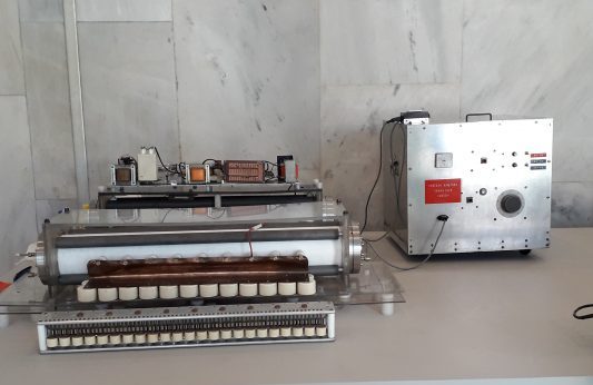
The device is a working station and consists of a molecular beam apparatus, a quadrupole mass spectrometer (Balzers QMG 311), (which can be operated on a “time of flight” mode if required), a molecular fluorine laser at 157 nm, and a data acquisition system.
The Balzers QMG 311 quadrupole mass spectrometer is a high resolution apparatus, able to cover the 0-300 a.m.u. range. The system consists of the control unit, the analyzer and the detection electronics. The analyzer is equipped with an electron impact ionization source in an open design and the detector is an off axis Secondary Electron Multiplier (SEM) differentially pumped. The signal is amplified with the system preamplifier (EP 511) and electrometer controller (QME 311) and processed with a PC computer acquisition system and software. The mass spectroscopy facility is extended with the ion polarity unit QMS 420 allowing positive and negative ions detection.
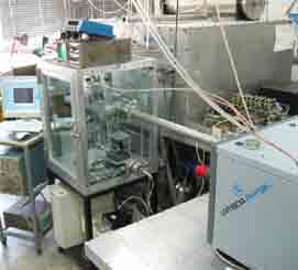
The VUV-micromachining working station is capable of processing different materials (from polymers to hard alloys) with 1μm resolution. A user-friendly software, (besides controlling the experimental parameters), has one additional degree of freedom that allows surface modification and processing with specified patterning. The main components of the system are: (1) The 157 nm laser (Lambda-Physik LPF 200). (2) The VUV high quality beam projection optics. (3) The computer control X-Y-Z-θ motorized stage, combined with one CCD imaging system for real time imaging and automatic control. The system is operating inside a shielded chamber in N2 environment. Applications include surface modification and functionalization of thin polymeric films for sensing and space applications and DNA chip manufacturing.
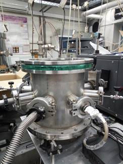
The pulsed laser deposition workstation is used to fabricate core-shell nanostructures (1-100nm) of hard intermetallic alloys. The main components of the system are: (1) The 157 nm laser (Lambda-Physik LPF 200). (2) The VUV high quality axial laser beam focusing optics. (3) The computer control X-Y-Z motorized stage bearing the substrate where the core-shells are grown. The system is operating at high vacuum conditions inside an all-stainless-steel chamber. High quality nano-structured core-shells, semiconductors and quazicrystals, have been synthesized with this configuration and applications include: (1) Investigation of the magnetic and electronic properties on nano-structures. (2) Development of new photonics systems with defined functionalization such as photovoltaics. (3) Hydrogen storage nano-materials from intermetallic alloys. (4) Quazicrystals, and (5) magnetic core-shells.
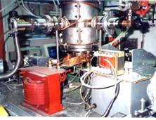
This is a lab-built device which allows mono-crystals of wide band gap dielectric crystals to be grown, with the Bridgman-Stockbarger method, from liquid melts after pulling of the seed crystal at temperatures as high as 15000C. Mono-crystals with dimensions 5 x 0.5 cm have been grown with this device. Good quality wide band gap fluoride dielectric crystals, doped with trivalent rare earth ions, can be developed due to an accurate temperature control during the pulling and cooling stages of the growth process.
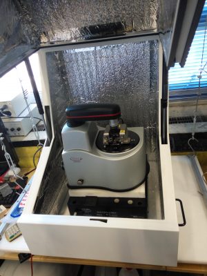
The Veeco di-Innova Scanning Probe Microscopy (SPM) provides high resolution scanning, and wide range of functionality for physical chemistry and materials science. It offers a fully complement of SPM techniques providing surface characterization of sample both in air and liquid, such as:
Contact Mode; Tapping Mode; Later Force Microscopy (LFM); Scanning Tunneling Microscopy (STM); Magnetic Force Microscopy (MFM); Phase Imaging; Conductive Atomic Force Microscopy (C-AFM); Scanning Thermal Microscopy (SThM); Force Distance Spectroscopy.
A closed-loop scanner (100 x100 μm2 and Z > 7.5 μm) or an open-loop scanner (5 x 5 μm2 and Z > 1.5 μm) are available.
The di-Innova system is placed on a vibration isolation table (K-Minus Technology).
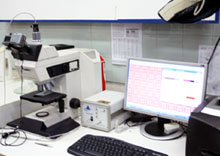
For optical imaging on the macro-scale, a metallographic optical microscope (Leica DMRX), equipped with digital cameras is used. The microscope can be used in polarized and phase contrast modes and is combined with a thin-film-thickness measuring spectroscopic reflectrometer, through a c-mount adapter in a simple configuration . The system enables thickness measurements from 10 nm up to 250 μm (400 μm) for a large number of materials (semiconductors, polymers, glasses, resists, metals, oxides etc) by analyzing white light interference This is a non-destructive technique and does not need any special sample preparation. Up to three layers can be analyzed in the film stack. It can be combined with the Leica DMRX optical microscope.
Pulse duration: 30ps
Wavelength :1064nm – 532nm – 355nm – 266nm
Max energy : 35mJ
Max repetition rate : 10Hz